Quick primer if you haven’t run into TinyTapeout before: it’s a project that lets individuals submit small custom digital (and now some analog) chip designs, usually written in Verilog or built visually in Wokwi, which then get fabricated for real on a shared silicon wafer alongside hundreds of other people’s designs. You get an actual physical chip back. It’s the closest thing hobbyists have to affordable custom silicon.
I went looking through the TTSKY26c shuttle, which closed submissions on September 7th with 242 designs, and one project stood out from the usual blinkenlights and 7 segment display demos: an S/PDIF to I2S receiver built by developer Jussi Kilpelainen. It’s real audio signal processing squeezed into a couple of silicon tiles, and I think it’s a genuinely clever piece of engineering.
What it actually does
S/PDIF is the format your CD player, game console, or older AV receiver uses to send digital audio over a single coaxial or optical cable. I2S is the format most audio chips, DACs, and codecs actually want to receive internally. This chip bridges the two entirely in hardware, no microcontroller involved.
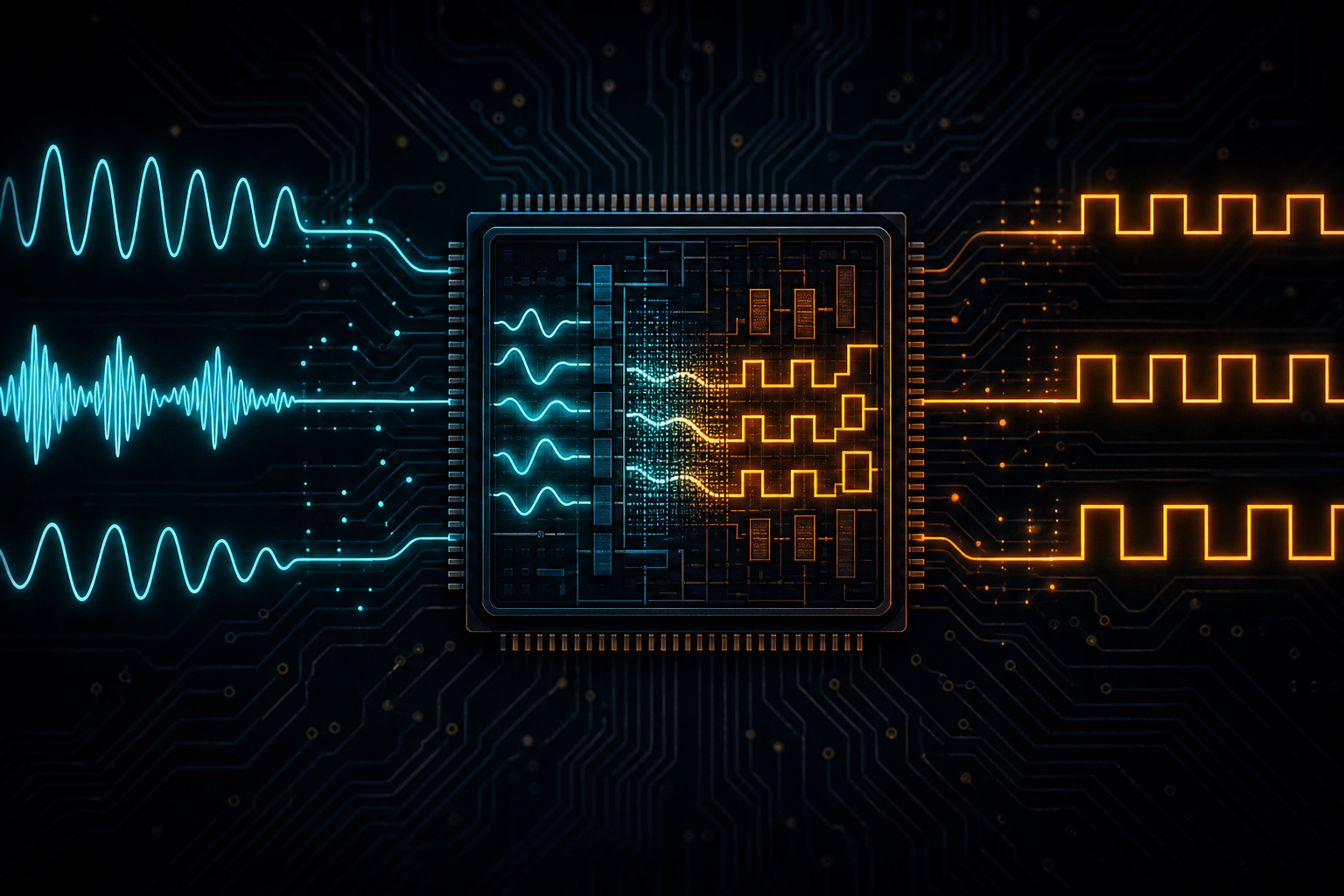
The clever part is clock recovery. S/PDIF doesn’t send a separate clock signal, the timing information is baked into the biphase mark encoding of the data itself. The receiver module oversamples the incoming signal with a free running 50MHz clock, measures the width of each transition, and classifies pulses as short, medium, or long to decode the biphase mark coding and lock onto the embedded clock. Once it’s synchronized, it regenerates a proper I2S bit clock and word select signal, spits out 24 bit left and right samples, and even downmixes to a mono PWM output through a simple 1-bit DAC for driving a speaker directly through an RC filter.
There’s also a genuinely nice touch buried in the pinout: an analog comparator input meant to be paired with an external RC network, so you can build a mute delay that prevents your amplifier from popping on and off between tracks when the signal drops momentarily. That’s a real world audio engineering detail, not something you’d think to add unless you’d actually built audio gear before.
What’s clever about it
Doing clock recovery entirely from a free running oversampling clock, with no external PLL or dedicated audio clock, is the kind of constraint that makes a small chip design actually interesting. Most people would reach for a PLL to lock onto the recovered clock cleanly. Instead, this design lets the recovered unit interval drive I2S generation directly, using a one deep double buffer to hand samples across clock domains, occasionally repeating or skipping a frame if the rates don’t align perfectly. It’s not bit-exact under clock drift, but it’s glitch-free, which is the right tradeoff for something meant to drive a physical DAC where a single dropped sample is inaudible and a stuck bit clock isn’t.
What I’d question
The repeated or skipped frame behavior under drift is a reasonable engineering compromise, but I’d want to see it characterized more rigorously. How often does it actually happen at real world clock tolerances, and is it audible on cheap consumer DACs with less forgiving analog reconstruction filters? The README doesn’t go deep on measured jitter numbers, which is understandable given this is a single tile hobbyist tapeout and not a commercial audio product, but it’s the first thing I’d want tested on real silicon once chips come back.
An alternative approach
The obvious alternative is using an actual PLL to lock onto the recovered S/PDIF clock and generate a clean, jitter filtered I2S clock from it, the way a commercial S/PDIF receiver chip like the CS8416 does. That buys you a bit-exact, low jitter output that professional audio gear would actually want. The cost is real: PLL design on an open shuttle process like SKY130 is nontrivial, eats more die area, and burns more of your power budget on a process that isn’t tuned for analog precision the way a dedicated audio silicon process would be. For a single tile hobbyist project with one shot at fabrication and no room for a redesign if the PLL doesn’t lock reliably, skipping the PLL entirely in favor of straightforward oversampling and a tolerant double buffer is the more pragmatic choice. It’s a smaller, more predictable design surface, and the failure mode (an occasional repeated sample) is a lot more forgiving than a PLL that doesn’t lock at all.
The project’s GitHub repository has the full source, though the README is still mostly the stock TinyTapeout template text as of this writing rather than a full writeup, so if you want the detailed module breakdown, the project page on tinytapeout.com has the more complete signal flow description and pinout table. Either way, this is a nice reminder that “tiny” silicon doesn’t mean toy projects. Real signal processing fits in a couple of tiles if you’re careful about what you’re willing to trade away.