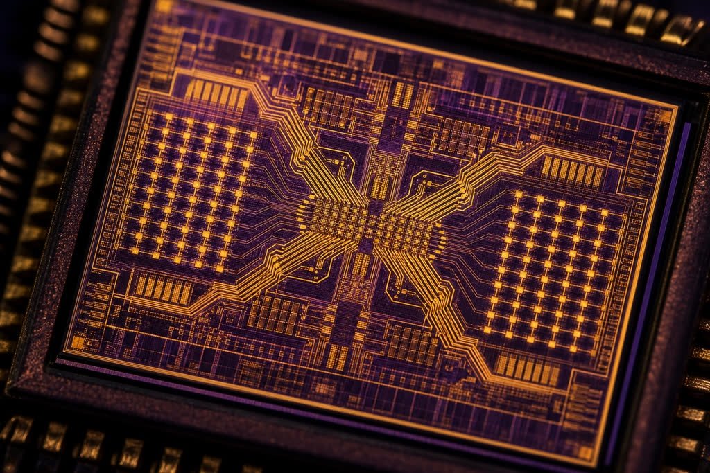
TinyTapeout is an open silicon shuttle project: anyone can design a small digital or analog chip, usually in Verilog or through the Wokwi web IDE, and get it fabricated for real on a shared silicon wafer alongside hundreds of other tiny designs from hobbyists, students, and researchers. Each design gets one or more “tiles” on the shuttle, and the whole thing gets manufactured and shipped back as working chips. I go looking through each new shuttle for something with real engineering substance, and the TTSKY26c shuttle had one that stood out immediately.
A team from RV College of Engineering in Bengaluru, working out of their Center of Excellence in Integrated Circuits and Systems, submitted a design called Crypto-Agile NTT Butterfly Unit. It fits into a single 1×1 tile and it does something I have not seen on a TinyTapeout shuttle before: it implements the core arithmetic building block for all three NIST post-quantum cryptography standards, ML-KEM, ML-DSA, and FN-DSA (Falcon), in one shared hardware datapath, with the scheme selectable at runtime rather than baked in at synthesis time.
What an NTT butterfly actually does
Post-quantum lattice cryptography leans heavily on polynomial multiplication over specific finite fields, and the Number Theoretic Transform is the standard trick for making that fast, the same way an FFT speeds up regular polynomial and signal multiplication. The “butterfly” is the basic repeated operation inside an NTT: take two values, multiply one by a fixed coefficient under a modulus, then add and subtract to produce two new values. You run thousands of these small butterfly operations to complete a full transform. If you are building real hardware for post-quantum crypto, the butterfly unit is the thing you end up implementing over and over, so making one fast, small, and correct actually matters.
The three standards this chip supports each use a different modulus: 3329 for ML-KEM, 8380417 for ML-DSA, and 12289 for Falcon. Normally that means three separate pieces of hardware, or a single piece of hardware that has to be redesigned per standard. This design instead uses a radix-2 bit-serial Montgomery multiplier, an approach that works correctly for any odd modulus, so switching schemes is just a mux flip on the modulus constant and a change to a counter’s terminal value. No separate reduction circuitry per scheme.
What is clever here
The area optimization is the interesting engineering decision. A single 1×1 tile on TinyTapeout is a tight budget, so the team time-shared one 25-bit three-operand adder across three different jobs: partial product accumulation during multiplication, Montgomery reduction correction, and the actual butterfly add and subtract. A control FSM sequences which job the adder is doing on which cycle. That is a classic hardware tradeoff, you are trading silicon area for extra clock cycles per operation, and it is exactly the right call when your area budget is one tile and your design goal is fitting three crypto standards into it. The repo’s own writeup claims no prior TinyTapeout submission has done PQC or NTT hardware at all, and skimming through past shuttles, that tracks.
I will be honest about my hesitation too: this only implements the butterfly arithmetic, not full ML-KEM or ML-DSA encryption or signing. It is the inner loop kernel, not a complete crypto engine. That is a completely reasonable scope for a single tile, but it means this chip alone does not do post-quantum encryption, it does the multiply-and-add step that a larger system built around it would call repeatedly. Worth knowing before you get too excited about it.
An alternative approach and its tradeoffs
Instead of time-sharing one adder across three functions, a more straightforward design would give each function, multiplication, Montgomery correction, and the butterfly add/subtract, its own dedicated adder. That would remove the FSM sequencing complexity and probably run faster in terms of latency per operation, since you are not waiting your turn for shared hardware. The tradeoff is area: three separate adders instead of one shared one would very likely have blown the 1×1 tile budget, forcing a 2×1 or larger tile allocation, using resources that could otherwise host another team’s project on the shuttle. Given TinyTapeout’s whole model is about fitting interesting designs into small shared silicon, the time-shared approach is the more appropriate choice here even though it costs some cycles.
If you want to see the chip map or browse other projects on this run, the shuttle page is at tinytapeout.com/chips/ttsky26c. The full source, docs, and test suite for this specific project are on GitHub at RVCE-ECE-Shylashree/Crypto-Agile-NTT-Butterfly, verified clean on DRC, LVS, and timing across all nine PVT corners, with cocotb tests checked against a Python golden model for all three schemes.